This blog post will serve as an overview of the processes that went into designing, implementing, and then actually deploying a transformer model onto a FPGA chip!
For brevity, I will skip out on all the prerequisite knowledge, might do a blog write up in the future. However, I learned most of this through HDLBits and the digital hardware course ECE627 at UWaterloo.
Here is a list of the topics I learned in order to do this project!
- Verilog syntax (Wires, logic, modules, behavorial and structural modeling)
- Synthesizing logic in verilog (Conditional execution, basic arithmetic operations, registers)
- State machines (Combinational logic + registers to create feedback, and implementing a logical state machine on hardware)
- Pipelining (Increase throughput, manage latency correctly, address bubbles, LUT usage tradeoff, identifying critical paths)
- Memory (Memory layouts, shared memories, read/Write arbitration with muxes)
- Tooling (Simulation, synthesis, implementation, timing analysis, resource analysis, waveforms, test benchs, etc)(Warning: FPGA tooling is frustrating!)
This project was deployed on a PYNQ FPGA board, which is a hybrid FPGA + ARM SoC (System-on-Chip) that allows you to run an embedded Linux stack on the ARM CPU and use the FPGA as an accelerator. PYNQ also also ships with user-friendly Python APIs which are useful for programming and interacting with the FPGA.
Part 1 - Architectural Design of Project
For this project, my primary goal was to implement a LLM on an FPGA device. Traditional BERT/Transformers based models use large floating-point arithmetic which are expensive to implement on a hardware level. Since FPGAs are relatively low powered devices (and usually used in an edge computing environment) compared to GPUs and ASICs, I did research on lightweight alternatives of the LLM architecture.
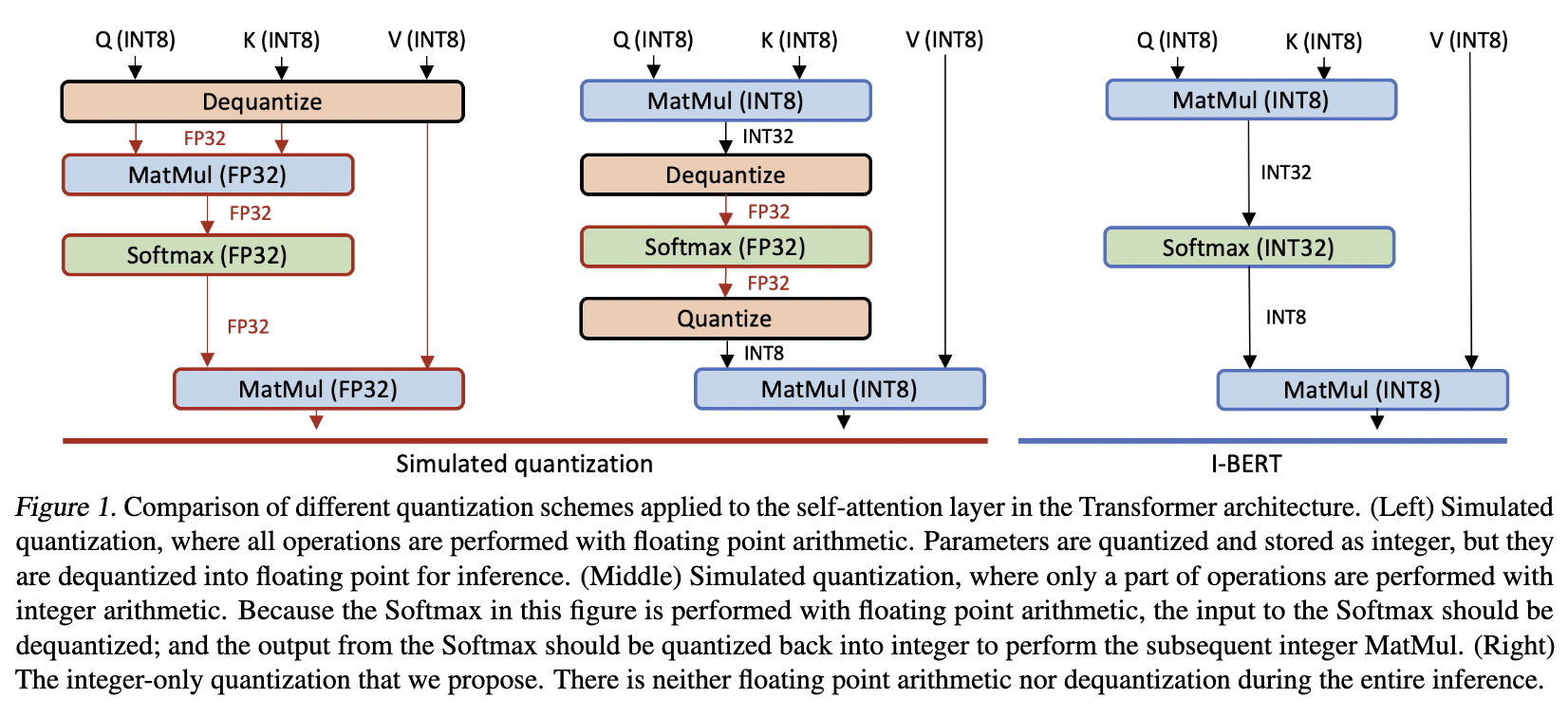
In order to adopt the transformer architecture to a lightweight environment, this paper "I-BERT: Integer-only BERT Quantization" proposes a fixed-point integer representation for all data-types and operations. Operations such as attention, layer normalization, softmax, GELU were all adapted to be done using only integers.
Here is a figure demonstrating the I-BERT quantization scheme.
Here are some sample python implementations of operations after I-BERT adaptation. These functions were used to simulate and validate the result of our system verilog modules.
Attention
def requant(qin: np.int32, bias: np.int32, m: np.int32, e: np.int8) -> np.int8:
'''
qin - int32, input
bias - int32, requantization multiplier
e - int8, requantization shifter
qout - int8, output
'''
qbias = qin + bias # int32
qm = np.int64(qbias) * m # int64
qout = np.round(qm * 2.0**(-e)) # int8
qout = np.int8(qout)
return qout
def attn_head(I: np.int8, Qw: np.int8, Kw: np.int8, Vw: np.int8,
Qb: np.int32, Kb: np.int32, Vb: np.int32,
Qm: np.int32, Km: np.int32, Vm: np.int32,
Qe: np.int8, Ke: np.int8, Ve: np.int8,
Cm: np.int32, Ce: np.int8) -> np.int8:
'''
I - int8, (64,768), input
Qw, Kw, Vw - int8, (768,64), weights
Qb, Kb, Vb - int32, (1,64), bias
Qm, Km, Vm - int32, (1,64), requantization multiplier
Qe, Ke, Ve - int8, (1,64), requantization shifter
Cm - int32, (1), requantization multiplier
Ce - int8, (1), requantization shifter
qout - int8, output
'''
I_Q = np.matmul(I, Qw, dtype=np.int32)
I_K = np.matmul(I, Kw, dtype=np.int32)
I_V = np.matmul(I, Vw, dtype=np.int32)
Q_8 = requant(I_Q, bias=Qb, m=Qm, e=Qe)
K_8 = requant(I_K, bias=Kb, m=Km, e=Ke)
V_8 = requant(I_V, bias=Vb, m=Vm, e=Ve)
S = np.matmul(Q_8, K_8.T, dtype=np.int32)
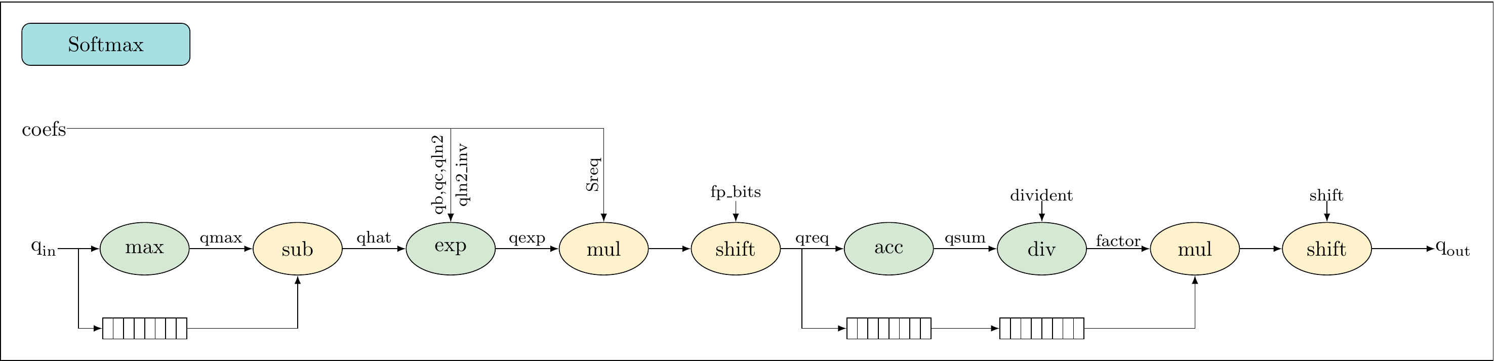
P = softmax(qin=S, qb=np.int32(1874), qc=np.int32(1338211),
qln2=np.int32(-480), qln2_inv=np.int32(-2236963),
Sreq=np.int32(26291085), fp_bits=30, max_bits=30, out_bits=6)
C_32 = np.matmul(P, V_8, dtype=np.int32)
C_8 = requant(C_32, bias=0, m=Cm, e=Ce)
return C_8Layer normalization
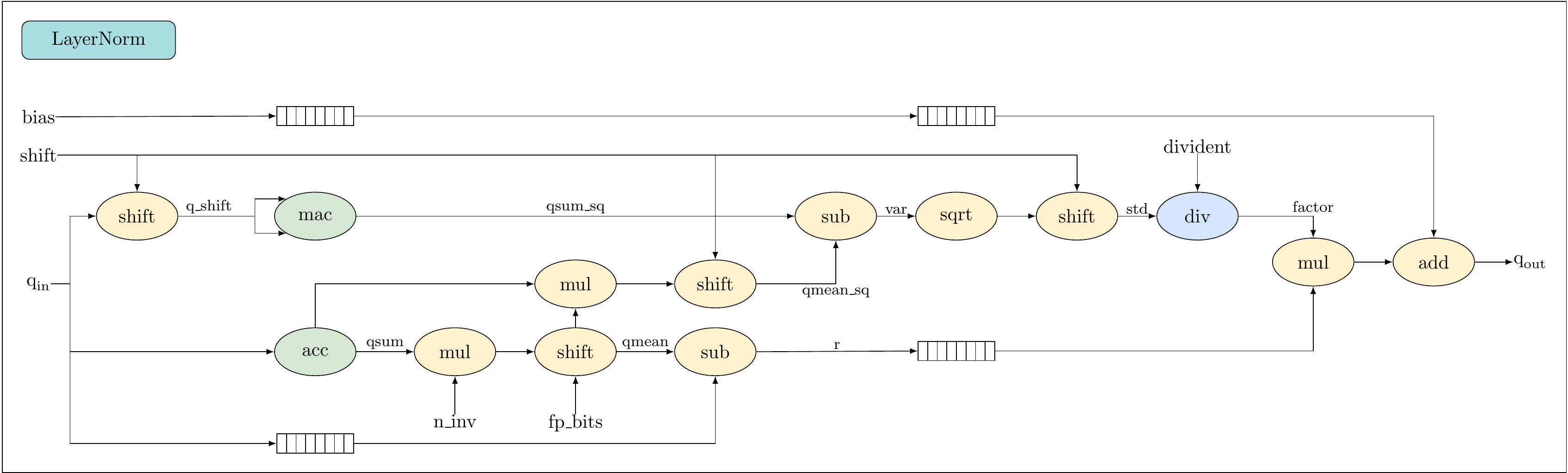
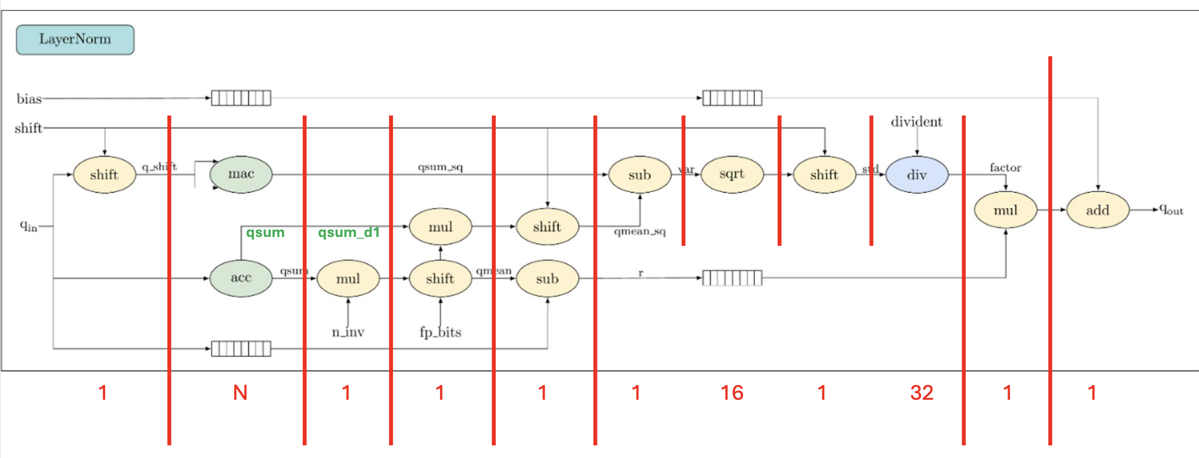
def layer_norm(qin: np.int32, bias: np.int32, shift: int=6,
n_inv: int=1398101, max_bits: int=31, fp_bits: int=30) -> np.int32:
'''
qin - int32, input
bias - int32, bias
shift - integer, shift amount
n_inv, max_bits - integer constants
fp_bits - constant, fixed point multiplication bits
qout - int32, output, integer layer_norm
'''
divident = 1 << max_bits
qsum = np.sum(qin, axis=-1, keepdims=True, dtype=np.int64) # int64, acc
q_shift = qin >> shift # int32, shift
q_sq = q_shift * q_shift # int32, hanled by mac
qsum_sq = np.sum(q_sq, axis=-1, keepdims=True, dtype=np.int64) # int64, mac
qmul = qsum * n_inv # int64, mul
qmean = qmul >> fp_bits # int32, shift
r = qin - qmean # int32, sub
qmean_mul = qmean * qsum # int64, mul
qmean_sq = qmean_mul >> (2 * shift) # int32, shift
var = qsum_sq - qmean_sq # int32, sub
var_sqrt = np.floor(np.sqrt(var)) # uint16, sqrt
var_sqrt = np.uint16(var_sqrt)
std = np.int32(var_sqrt) << shift # int32, shift
factor = np.floor(divident / std.astype(np.float64)) # int32, div
factor = np.int32(factor)
qout_mul = np.int32(r * factor) # int32, mul
print(qout_mul[0][:5])
qout = (qout_mul >> 1) + bias # int32, shift, add
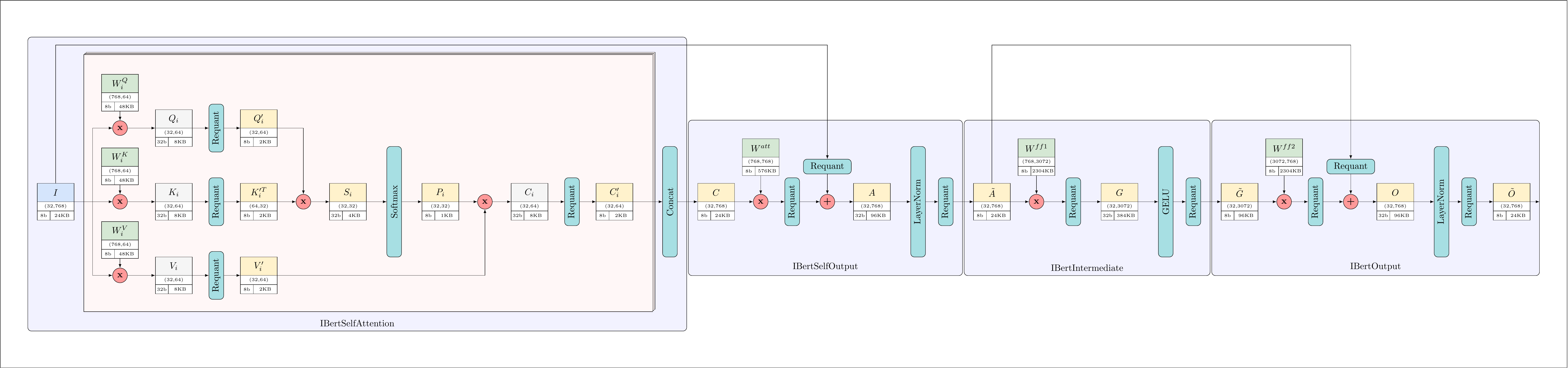
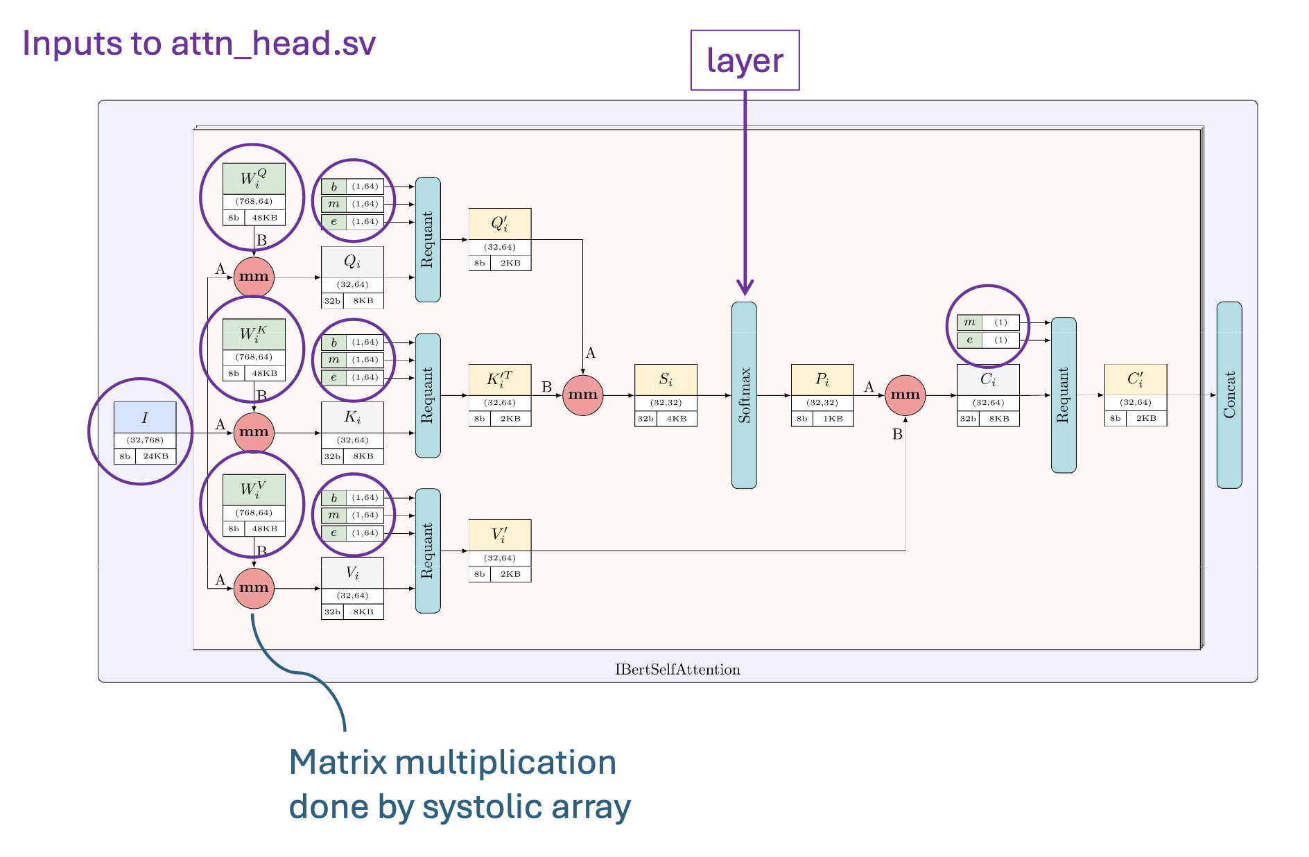
return qoutThis diagram shows the final architecture and datapath of the hardware modules we are going to implement (Labeled with datawidth and weight size).
Part 2: Implement and design submodules in System Verilog
Now on to the fun part, we have to design the hardware architecture to carry out the computation within our architecture, and then implement them in system verilog! Our core acceleration strategy is leverage the systolic array microarchitecture to carry out matrix multiplications. (Tensor core's hardware architecture, I might do a future write up on why it is so efficient from a hardware perspective)
Basic computation blocks
Unlike software, in hardware we have to manually define, design, and implement all basic mathematic operations. A lot of these operations take a varied number of cycles to complete depending on input, and require carefully pipelining of the computation to ensure timings are met!
The following modules were implemented (Hyperlinked with the files)
- mac: multiply accumulate
- div: integer division, implemented with a state machine
- exp: exponentiation, 7 state input pipelining
- sqrt: square root
Here are some helper important modules I implemented
- lopd: leading one position detector, equivalent to floor(log2(x)), hardcoded with a mux
- sreg: Shift register
- fifo: FIFO queue
Systolic array
Implementing a systolic array is sort of a 3 step process. We need to 1. Setup infrastructure for data movement between the ram banks on the FPGA and hardware modules 2. Design control logic modules for address generation (Think Nvidia's TMA) 3. Implement the core systolic array.
For part 1, in order to move data from RAM banks to the FPGA, we use AXI (Advanced eXtensible Interace) which is a on-chip communication bus protocol for ARM chips. We simply have to implement a system verilog module that follows the master-slave protocol which involves the following
- Setting up the five channels for read write operations (AR, R, AW, W, B)
- Handshaking with VALID/READY signals for each channel
- Synchronization and control for burst-transfer signals
- Unpacking/packing data, utilize ping-pong buffering for improved throughput
These logic were implemented in the following files:
- stream_vector_mem: Define standard AXI stream interface definitions, responsibile for handshake and control signals
- s2mm: stream to memory memory mapped data path (store AXI stream in Block-RAM)
- mm2s: the reverse, these two files handle data packing and unpacking
Now for part 2, we have to implement the core systolic array logic.
A systolic array is a 2D grid of simple computing elements connected to each other in nearest neighbour fashion.
Dataflow through the array proceeds in a systolic fashion (one hop at a time), new elements injected into the array from the left (A) and top (B) flanks per cycle.
The co-ordination of data injection is crucial for correct evaluation of the computation. Each processing unit performs multiply-accumulate operation on streaming inputs.

In terms of code, this is actually really simple to implement.
pe.sv
`timescale 1ps / 1ps

module pe
#(
    parameter integer D_W     = 8,      // operand data width
    parameter integer D_W_ACC = 32      // accumulator data width
)
(
    input  logic                      clk, rst, init, in_valid,
    input  logic signed [D_W-1:0]     in_a, in_b,
    input  logic signed [D_W_ACC-1:0] in_data,
    output logic signed [D_W-1:0]     out_a, out_b,
    output logic signed [D_W_ACC-1:0] out_data,
    output logic                      out_valid
);

logic signed [D_W_ACC-1:0] acc_reg;
logic signed [D_W_ACC-1:0] in_data_reg;
logic                      valid_reg;

always_ff @(posedge clk) begin
    if (rst) begin
        // set everything to 0
    end else begin
        out_a <= in_a;
        out_b <= in_b;
        in_data_reg <= in_data;

        if (in_valid) begin valid_reg <= 1;
        end else begin valid_reg <= 0; end

        if(init) begin
            out_data <= acc_reg;
            out_valid <= 1;
            acc_reg <= in_a*in_b;
        end else begin
            out_data <= in_data_reg;
            out_valid <= valid_reg;
            acc_reg <= acc_reg + (in_a * in_b);
        end
    end
end
endmodule
systolic_array.sv
`timescale 1ps / 1ps

module systolic
#(
    parameter integer D_W     = 8,      // operand data width
    parameter integer D_W_ACC = 32,     // accumulator data width
    parameter integer N1      = 8,
    parameter integer N2      = 4
)
(
    input  logic                      clk,
    input  logic                      rst,
    input  logic        [N2-1:0]      init [N1-1:0],
    input  logic signed [D_W-1:0]     A    [N1-1:0],
    input  logic signed [D_W-1:0]     B    [N2-1:0],
    output logic signed [D_W_ACC-1:0] D    [N1-1:0],
    output logic        [N1-1:0]      valid_D
);

// write your code here

logic signed [D_W-1:0]     pe_a     [N1-1:0][N2-1:0];
logic signed [D_W-1:0]     pe_b     [N1-1:0][N2-1:0];
logic signed [D_W_ACC-1:0] pe_data  [N1-1:0][N2-1:0];
logic                      pe_valid [N1-1:0][N2-1:0];

genvar i, j;
generate
    for(i = 0; i < N1; i++) begin : ROW
        for(j = 0; j < N2; j++) begin : COL

            if (i == 0 && j == 0) begin : bothzero

            pe #(.D_W(D_W),.D_W_ACC(D_W_ACC)
            ) pe_inst(
                .clk (clk), .rst (rst), .init (init[i][j]),
                .in_a       (A[i]),
                .in_b       (B[j]),
                .in_data    (0),
                .in_valid   (0),
                .out_a (pe_a[i][j]), .out_b (pe_b[i][j]), .out_data   (pe_data[i][j]), .out_valid  (pe_valid[i][j])
            );
            end else if(i == 0) begin : izero
            pe #(.D_W(D_W),.D_W_ACC(D_W_ACC)
            ) pe_inst(
                .clk (clk), .rst (rst), .init (init[i][j]),
                .in_a       (pe_a[i][j-1]),
                .in_b       (B[j]),
                .in_data    (pe_data[i][j-1]),
                .in_valid   (pe_valid[i][j-1]),
                .out_a (pe_a[i][j]), .out_b (pe_b[i][j]), .out_data   (pe_data[i][j]), .out_valid  (pe_valid[i][j])
            );
            end else if(j == 0) begin : jzero
            pe #(.D_W(D_W),.D_W_ACC(D_W_ACC)
            ) pe_inst(
                .clk (clk), .rst (rst), .init (init[i][j]),
                .in_a       (A[i]),
                .in_b       (pe_b[i-1][j]),
                .in_data    (0),
                .in_valid   (0),
                .out_a (pe_a[i][j]), .out_b (pe_b[i][j]), .out_data   (pe_data[i][j]), .out_valid  (pe_valid[i][j])
            );
            end else begin : neitherzero
            pe #(.D_W(D_W),.D_W_ACC(D_W_ACC)
            ) pe_inst(
                .clk (clk), .rst (rst), .init (init[i][j]),
                .in_a       (pe_a[i][j-1]),
                .in_b       (pe_b[i-1][j]),
                .in_data    (pe_data[i][j-1]),
                .in_valid   (pe_valid[i][j-1]),
                .out_a (pe_a[i][j]), .out_b (pe_b[i][j]), .out_data   (pe_data[i][j]), .out_valid  (pe_valid[i][j])
            );
            end

            if (j == (N2-1)) begin : setoutput
                assign D[i]       = pe_data[i][j];
                assign valid_D[i] = pe_valid[i][j];
            end
        end
    end
endgenerate

endmodule
Now for the last part, in order for the systoilc array to compute matrix multiplication correctly, it needs to be fed the inputs in a correct manner. This image illustrates the indexing of values fed into each row/column. The matrix A will be streamed from the left of the 4x4 systolic array in a row-wise fashion. The matrix B will be streamed from the top of the 4x4 systolic array in a column-wise fashion.

The input and output matrices for the matrix-multiplication are stored in RAM banks.
- Matrix A is partitioned row-wise across the banks and each row is fed serially into the in_a port of the systolic.sv module. The AXI stream suppling the A matrix provides this data in row-serial fashion with elements supplied from top-left to bottom-right corner of the matrix one item per cycle.
- Matrix B is partitioned column-wise across the banks and each column is fed serially into the in_b port of the systolic.sv module. Even though B is read in column-wise fashion when entering the systolic array, it is supplied by the external world in row-serial fashion. The reason becomes clear when we have to cascade multiple systolic arrays together for the IBERT Attention Head.
- Matrix D is stored just like matrix A in row-wise fashion across the banks. The systolic array output is streamined into the banks in row-wise fashion from the out_d port in systolic.sv. The AXI output stream that supplies D to the next stage of computation, or back to the ARM host, does so in row-wise fashion as well.
Here are the files implemented
- mem_write_A.sv will generate the sequence of write addresses for each memory bank storing A.
- mem_write_B.sv will generate the sequence of write addresses for each memory bank storing B. This is slightly tricky as you have to do a row/column permutation
- mem_read_D.sv will generate the sequence of read addresses for each memory bank storing D.
Part 3: LSI - Stitching modules together for top level assembly
Now that we have all these base modules completed, we can perform top level assembly and stitch them together into higher level usable modules like mm (matmul), mm_gelu (matmul gelu fusion), attn_head (full self attention computation), and then instantiating these higher level modules to define the chip layout with necessary clock generators.
Implementing base modules into useful algorithms, namely in our case gelu, matmul, and layer_norm.
- mm.sv: combining systolic with memory interfaces and address generators
Stitching together algorithms into transformer components
- attn_head.sv
- mm_ln.sv
- mm_gelu.sv
For high level synthesis, it is important to pipeline inputs and setup proper buffering between stages in order to maintain throughput. Here is an example of how you would have to separate layer norm into stages.
Part 4: Verification, Synthesis and Implementation
After implementing all core system verilog modules, we have to step through the typical digital design lifecycle in order to deploy the code. This consists of
- Verification: Ensures the code accurately implements the intended functionality, done through simulation software such as xsim (vivado proprietary) or verilator (open source)
- Synthesis: Convert the RTL code to a gate-level netlist, a description of the circuit in terms of basic logic gates and wires, and check for timing performance, power consumption, and silicon usage, for AMD chips this has to be done on xsim
- Implementation: Generate a physical design from the gate-level netlist, Vivado's xsim can do this automatically which saves the effort of manual placement and routing
Essentially, at each stage you unlock a new granularity of testing. Verification is fastest and ensures correct logic (and assumes no propagation delay). Synthesis verification tests that you're simulation waveforms match expected once you account for the delay models of each gate/component, Implementation simulation is the slowest simulation of the final netlist after place-and-route which simulates the entire chip including gate/component + routing delays.
Since Vivado's software suite can do synthesis and implementation automatically, verification is the only step we have to do manually. This consists of writing a specific test bench for each module, which feeds the module data and compares the output against our reference python implementation.
For synthesis and implementation, we simply have to run the Vivado software on our modules. Note that this is not always trivial as there are different assumptions made on the System Verilog code at each stage. Small modifications in the code may be required at each stage to create the same logic.